CASPA Quarterly Special Interest Group Seminar
Date: Jan. 30, 2021 Sat. 5pm – 6:30pm
Topic: Semiconductor Package and Testing, the State of the Art
Registration: click here!
Event Zoom link: https://zoom.us/j/91086755359
Event Broadcast link: click here!
Agenda:
5:00pm – 5:05pm Welcome remark from Ian Wang, Head of Symposium, CASPA
5:05pm – 5:10pm CASPA Introduction by Xiaodong Zhang, President of CASPA
5:10pm – 5:45pm The Future is Heterogeneous Integration
– Dr. William Chen, Senior Fellow, ASE (slides)
5:45pm – 6:20pm Packaging Fundamentals of High Performance Applications
– Mr. Yaojian Lin, Vice President, JCET (slides)
6:20pm – 6:40pm Panel discussion
Speakers:

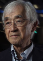
William Chen, Senior Technology Fellow, ASE USA
Speech Title: The Future is Heterogeneous Integration
Semiconductor technology is fueling the digital transformation that is increasingly being used to solve some of the world’s greatest challenges. Our connected lives generate 2.5 quintillion bytes of data daily, driving unprecedented demand for bleeding edge digital networks, connectivity, storage, memory, edge to cloud compute, and so much more.
Heterogeneous Integration refers to the integration of separately manufactured components into a higher-level assembly (System-in-Package, known as SiP) that in the aggregate provides enhanced functionality and improved operational characteristics. It is now the key technology direction going forward, driving the pace of advancement for greater intelligence and connectivity, higher bandwidth and performance, and lower latency and power per function, all at a more manageable cost.
During his presentation, Dr. Bill Chen will introduce the heterogeneous integration roadmap, describing how broad ecosystem collaboration is positioning the industry to initiate a new era of technological and scientific advances to continue and complement scaling into the future.
Speaker Bio:
Dr. William (Bill) Chen is chief architect for technology strategy, lead mentor, and hands-on engineer for strategy implementation at ASE Group, blazing the trail for packaging innovators and innovation across the electronic industry ecosystem. His strategy portfolio includes SiP, copper wire-bond, 2.5D packaging, & fan-out wafer-level packaging, all game-changing technologies brought to high volume production to address new demands for emerging applications in IoT, cloud computing, autonomous automotive, AI and smart mobility.
Previously, Bill spent over thirty-five years at IBM, where he pioneered the concept and implementation of predictive verified modeling incorporating materials science, micromechanical, and finite element for design and manufacturing benefiting generations of packaging products, from BGAs to mainframe systems.
Bill is a past president of the IEEE Electronics Packaging Society and was the co-chair of the Packaging & Assembly TWG at ITRS until its closure by SIA in 2016. He now chairs the Heterogeneous Integration Roadmap, co-sponsored by three IEEE Societies (EPS, EDS & Photonics) together with SEMI and ASME EPPD. He is the recipient of IEEE Electronics Packaging Technology Field Award and ASME InterPACK Award. Besides being ASE Fellow, he has also been elected IEEE Fellow and ASME Fellow. Living by his motto, “Challenge things difficult but worthwhile”, Bill hopes to inspire more young engineers to always maintain an enthusiastic attitude while facing challenges, which once overcome, will sustain the prosperity and impact of the semiconductor industry.

Yaojian Lin, VP of Engineering and General Manager of R&D Center, JCET Group
Speech Title: Packaging Fundamentals of High Performance Applications
• Si node technology in IC scaling is becoming too expensive, and associated yield can be problematic, and moreover each node does not seem to provide the proportional performance and power benefits. In this context, the advanced packaging options have been surfaced out as an alternative. One option is to integrate heterogeneous dies in an advanced package, which can be called ‘chiplets’. From the OSAT standpoint, this chiplets is part of multi-die processing.
• Widespread adoption of 2.5D in price-insensitive markets such as chips for servers and network switches. On the other hand, fan-out option can be a much simpler approach to heterogeneous integration than 2.5D in that chips basically can be pushed closer together on a board and then packaged.
• In this talk, the fundamental processes to be considered can be discussed.
Speaker Bio:
Mr. Yaojian Lin, VP and General Manager of R&D Center, JCET Group. He has a bachelor’s degree from Huazhong University of Science and Technology, a master’s degree from Shanghai Jiaotong University, and a master’s degree from the University of Rochester. Currently, he is in charge of the China R&D Center of JCET Group , focusing on core customer technical support such as advanced assembly technology and product development, and has more than 100 US patents in the field of advanced packaging.