In wake of the rising of semiconductor testing market, CASPA, the largest Chinese American semiconductor professional association worldwide. We plan to organize a seminar discussing the technology trend in Semiconductor Testing. We are very pleased to invite you to speak at our 2022 Special Interest Group Seminar-II, scheduled on Saturday June 4th 4:00pm to 6:30pm on the internet via Zoom. This is part of CASPA technology forums organized throughout the year.
Eventbrite register Link https://caspa2022-sigii.eventbrite.com
Zoom meeting Link: https://us06web.zoom.us/j/86710279631?pwd=Wm9oT2I0aU9JTGo5Qjd4aHhic01BUT09
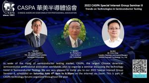
| 2022 CASPA Special Interest Group Seminar II
Trends on Technologies in Semiconductor Testing |
|
| 4:00pm – 4:05 pm | Welcome Remarks by CASPA Symposium Head |
| 4:05pm – 4:10pm | Introduction of CASPA by CASPA President |
| 4:10pm – 4:45pm | Mr. Sonny Banwari,
VP, Advantest Cloud Solutions, Advantest Corporation Hyper-Edge Computing and AI/ML drives high yields and quality of advanced packaging for chiplets |
| 4:45pm – 5:20pm | Dr. Zhongtao Fu ,
Chief Architect, HYC Technology ATE technology must keep up with the evolving IC technology |
| 5:20pm – 5:55pm | Mr. Peter Peng
Founder, Chairman & GM HISEMI ELECTRONICS TECHNOLOGY Co., Ltd Explore the Future Development Trend of IC Packaging and Testing Technology |
| 5:55pm – 6:30pm | Panel Discussion |
| 6:30pm | Closing Remarks |
Speaker #1

Mr. Sonny Banwari
VP, Advantest Cloud Solutions,
Advantest Corporation
Bio:
Mr Sonny Banwari is the VP of global business development and operations for Advantest Cloud Solutions (ACS) – a division of Advantest Inc. He has 30 years of international leadership experience upto level of VP/COO/President including 20 years in US and 10 years in Asia in semiconductor manufacturing and product development/validation supporting automotive, consumer, computing. Military/aerospace, communications, networking and industrial applications. He has delivered top results in positions of increasing responsibility at Fortune500 companies like Intel Corp (20 yrs) and Onsemi (7yrs) and other midsize companies including AT&S Gmbh and Advantest. He is a multi-lingual with English, Hindi, Japanese, and Spanish and beginner German/Mandarin. He enjoys a high profile in Asia and US technology sector and is board member of Industry associations in China, India and Philippines. He has a MS in Electrical Engineering from Arizona State University and MBA. He has also completed MIT coursework on Artificial Intelligence.
Speech Title:
Hyper-Edge Computing and AI/ML drives high yields and quality of advanced packaging for chiplets
Abstract:
Semiconductor test, like many industries, is experiencing a data revolution. With unprecedented demand for electronics of ever higher complexity, and in the face of a bend in the curve of Moore’s Law, manufacturers are moving to a chiplet-based paradigm. These products enable us to cram incomprehensible numbers of components into a growing array of products, resulting in the world’s total output of a staggering 1.6×10²¹ transistors in 2021 according to VLSI Research. All those components must be tested, and the corresponding amount of test data would meet any reasonable definition of “Big Data”. Compounding the problem, the sources of data feeding the test process are becoming more diversified, and traditional production electrical data is being augmented with equipment metadata, optical inspection data, on-chip lifecycle management data, and others, limited only by our collective creativity.
In this presentation, we describe data analytics-related trends that we observe in the industry. We elaborate the challenges that we see such as high-performance real-time decision-making in test operations and IP and data security across a disaggregated supply chain. We will give some specific examples of collaborative solutions being developed by Advantest and a wide ecosystem of analytics partners to address these issues including adaptive test solutions at parametric (e-test) and production test and show how they solve real industry problems and result in significant improvements in product decision-making, test cost, yield and capacity (the last two critical in the time of industry-wide shortages). We conclude with observations about what we see as crucial next steps including university and consortium collaboration to support the open solution ecosystem needed for success.
Speaker #2
Dr. Zhongtao Fu
Chief Architect,
HYC Technology
Bio:
Dr. Fu leads HYC Semiconductor division on a path to provide solutions for global semiconductor industries of IC and system test. He is responsible for identifying new technologies, as well as developing foundational technology capabilities in support of the current and future needs of IC manufacture, and packaging test customers. He has built the first ever Automated Test Equipment for HYC semiconductor division. He led the team and developed the most widely deployed tester in the quantity of thousands, Battery Management System tester, which was acknowledged as the most critical to the success of HYC in 2019. Recently, he architected the RF tester, TS1800, deployed in three major RFIC manufacturing test floors, winning the most Advanced Technical Award of JiangSu Province.
Previously at Maximum Integrated, as a Senior Staff Engineer, he was responsible for the company’s audio amplifier testing, including Fab Sort and Assembly Test.
Previously at Intel, as a senior engineer, Dr. Fu worked on the Etest metrology development. He has also acknowledged by pathfinding design and validation on the High Current Digital Power Supply for Intel’s test technology platform, High Density Modular Test (HDMT).
Dr. Fu has also contributed to advancing the field of mixed signal VLSI design and semiconductor technology. He published more than 20 peer reviewed papers.
Dr. Fu received his PhD from Cornell University, Ithaca, NY and Bachelor of Science degrees in Telecommunication Engineering from Hefei University of Technology, China.
Speech Title:
ATE technology must keep up with the evolving IC technology
Abstract:
Driven by the evolution of new technologies, highly integration of electronic components and the greater complexity of new devices, the growth in ATE market is expected. The Semiconductor Automated Test Equipment (ATE) market in the U.S. is estimated at US$1.1 Billion in the year 2020. China, the world`s second largest economy, is forecast to reach a projected market size of US$822.7 Million by the year 2027. Manufactures require fast time-to-market, low-cost and high yield to be successful in the ever-competitive market segment. HYC ATE is designed to meet China’s rapidly growing semiconductor industry, providing fast and highly reliable test results.
Speaker #3
Mr. Peter Peng
Founder, Chairman and General Manager,
HISEMI ELECTRONICS TECHNOLOGY Co., Ltd.
Bio:
Mr. Peter Peng, is the Founder, Chairman and General Manager of HISEMI Electronic Technology Co., Ltd., located in Chizhou, Anhui, China. He has 25 years of experience in semiconductor packaging and testing industry. He led his team to successfully accomplish the R&D of Anhui Provincial flat SIP packaging design and application project. In 2020, he completed the construction and production of the first DFN/QFN medium and high-end and SIP system level packaging and testing production line in the province, which makes HISEMI a new benchmark in semiconductor packaging and testing industry in China.
Prior to his current role, he worked at Sanyo Electric as an engineer, focusing on power management and motor drive chip research and development.
Mr. Peng served as the vice president of Anhui Semiconductor Industry Association and president of Chizhou Semiconductor Industry Association.
Speech title:
Explore the Future Development Trend of IC Packaging and Testing Technology
Abstract:
At present, the traditional packaging and testing technology in the global semiconductor industry is in parallel with the advanced packaging and testing technology. LGA, QFN, BGA and other mainstream traditional packaging technologies will carry out large-scale production. In the future, the development of new packaging technologies will evolve towards systematization and functionalization, realizing that more pins can be accommodated in a smaller packaging area, integrating multiple functional chips, reducing the size of modules, and improving the overall functionality and flexibility of the chip system. In the future, relying on advanced packaging and testing technology, we can further realize volume miniaturization and achieve heterogeneous integration of all semiconductor technologies.